History of the Chiplet – And Why it is the Future
Microchips have been around since the late 1950s, and have been a byword for cutting edge technology ever since. But it seems that the era of the monolith do-it-all chip is coming to an end, and the age of the chiplet has arrived.

Here we break it all down, from how chips have evolved over the last 60 years, to where we are now, and the role that Kandou’s innovative GlasswingTM technology has to play improving our data-driven future.
Moore’s Law
In 1965 Intel Co-founder Gordon Moore made a now very famous prediction: that every two years the number of transistors on a microchip would double at the same manufacturing cost per silicon area, accelerating the power and capabilities of the average computer, whilst also bringing the cost to consumers steadily down.
This prediction became known as Moore’s Law, and by and large he has been vindicated right up until the last few years. (Moore’s Law has been cited as one of the most influential sentiments guiding modern innovation.) Just as he suggested, the Intel 4004 (4-bit, 16-pin) in 1971 had 2,250 transistors, and a 10,000nm process, across 12 mm2. By 1974 Intel’s 8080 (8-bit, 40-pin) chip had 6,000 transistors, 6,000nm on a 20mm2 chip. This trend continued right up until the early 2020s.
But the world’s leading electronics minds are all largely in agreement. That law has had its day. There are now so many transistors (134bn on Apple’s 2023 M2 Ultra dual chip module) that verifying the design takes too long. Ensuring that they are 100% bug free is around 80% of the total cost. It’s just too much time, and too much effort.
So where do we go from here? Answer: Chiplets!
Chips vs chiplets. What’s the difference?
Moore predicted this too. In a small paragraph of his seminal 1965 paper “Cramming More Components Onto Integrated Circuits” he predicts the end to his Law, and offers an alternative out of the impasse:
“It may prove to be more economical to build large systems out of smaller functions, which are separately packaged and interconnected. The availability of large functions, combined with functional design and construction, should allow the manufacturer of large systems to design and construct a considerable variety of equipment both rapidly and economically.”
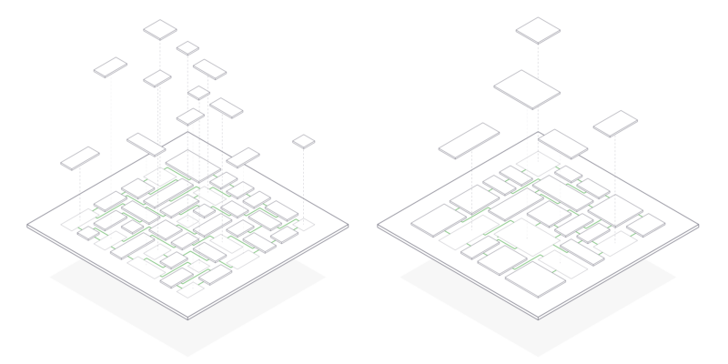
He suggests ultimately splitting the chip up into smaller pieces, with each ingredient dedicated to a different function. This essentially means that you don’t need all IP to be designed and integrated on the same process node. Instead one chiplet can be bleeding edge, while the rest can be derived from existing, established and verified IP.
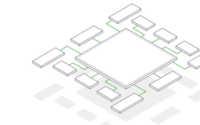
While a chip has its own package around it, chiplets don’t. The idea is that you create a bespoke shared package and connect the chiplets all together to do the same job a monolith chip would. This isn’t without its downsides, performance isn’t good because the distribution of functions adds latency, but the right architecture can offset this so the pros outweigh the cons.
Size counts
When you hear the word ‘chiplet’, it’s natural to think ‘so like a chip, but smaller’. Which isn’t entirely true.
It’s widely acknowledged across the industry that taping out a chip on advanced process nodes is getting harder and more expensive. Kandou manufacturing partner TSMC have recently announced that their 3nm wafer is going to be 25% more expensive than their 5nm wafer. To put it crudely, the more technology nodes advance the more costs go up.
A monolithic chip uses a smaller amount of real estate, but – as well as being costly to develop because of the time required – the type of area that it consumes is more expensive too.
Advanced process node is very expensive per square millimeter. So let’s say you have a 10mm by 10mm chip in 3nm technology. Compare that to cutting it up in four or five pieces, most of them in a previous process node – the cost of multiple chiplets is way smaller than the cost of the amount of a section. The surface area is larger, but the cost is less.
Chiplets benefit everyone
This unpackaged chiplet logic accelerates development time, so commercial companies can get products to market quicker. As Kandou’s Founder Dr Amin Shokrollahi says in this interview with Semiconductor Engineering “If you have an analog component in your design, there’s absolutely no point shrinking the process… it’s just costs and headache. So why don’t you just keep it with SerDes, and shrink the part that you want?”
Which is exactly what Amin and the team did to create GlasswingTM originally, collaborating with a tech infrastructure specialist to create chiplets that would enable them to get new products to market much faster than they could with a monolith.
Architectural redundancy typically increases reliability, a key priority for environments such as aerospace and defense, where troubleshooting and repairs are, for want of a better word, awkward.
Chiplets are also much more predictable – offering ‘fit and forget’ simplicity – which is ideal for datacenters and hyperscalers.
But the really interesting issue with the Chiplets is configuration – how you choose to stick them together. Versatility is what makes chiplets such an exciting premise – especially since you can combine novel designs with pre-existing ones – and being able to build a bespoke configuration opens up a world of possibilities. And this is where Kandou’s Glasswing shines.
What makes Glasswing special?
Created in 2016, Glasswing is an interconnect for chiplets. Designed using Kandou’s trademark mathematical insights, Glasswing offers very low power consumption, very high bandwidth, exceptional reliability and simple integration.
Most importantly, it supports long complex traces like zig-zag and horse-shoe, of different widths, just as you would see on a large printed circuit board. So instead of needing to sit in neat rows, far more chiplets can be integrated into an ecosystem in more complex ways.

This is enabled by Kandou’s unique CNRZ-5 Chord™ technology which is key to lower power using fewer pins, without sacrificing margin. So even though a chiplet isn’t proximal there’s no loss of signal or latency penalty.
So as Moore’s Law becomes consigned to the history books, chiplets allow you to keep pushing the envelope with your configuration and package designs – with Glasswing and Chord™ Signaling helping you push the furthest.


